PCB Solutions
Driven by your desire to achieve more, we have been constantly looking to break ground today technically and cost effectively
We offer you:
- Low to high layer counts: Single sided to 28 layers
- Complex PCB solutions: Special materials, heavy copper
- Quickturn Prototype
- Design for manufacturability (DFM)
- Global support
The Power behind
Your Global
PCB Solutions
Topsearch Printed Circuits Capabilities
|
Item
|
Production
|
Prototype
|
| Max Layer Count | 18 | 28 |
| Max Board Thickness | 0.175″ | 0.200″ |
| Min Board Thickness | 0.010“ | 0.008″ |
| Max Working Panel Size | 21″ x 24″ | 24″ x 26″ |
| Drill to Metal | 0.007“ | 0.006″ |
| Min drill diamater | 0.008″ | 0.006″ |
| Innerlayer Registration | +/- 0.003″ | +/- 0.002″ |
| Line Width/Spacing, Outer/Inner (17 micron) | 0.003″ / 0.003″ |
0.0025″ / 0.0025″ |
| Aspect Ratio | </=12:1 | </= 14:1 |
| Min QFP Pitch (not HASL) | 0.016″ | 0.010″ |
| Controlled Impedance(Single ended) (Differential) |
50 – 90 ohms +/- 8%* 100 – 155 ohms +/- 10%* |
50 – 90 ohms +/- 8%* 100 – 155 ohms +/- 8%* |
| Max Internal Copper Wt. | 6 oz | 12 oz |
| HDI(2+N+2 Max Layer Count) -Min Via Size – Min Capture Pad Size |
0.004″ 0.012″ |
0.004″ 0.012“ |
* Less than 10% impedance tolerance capability is design dependent.
|
High Performance materials
|
Production
|
Prototype
|
| Bismalemide Triazine (BT) or equivalent |
Yes
|
Yes
|
| Nelco N – 4000 – 13 (SI) |
Yes
|
Yes
|
| Nelco N – 4000 – 13 |
Yes
|
Yes
|
| Getek / Megtron |
Yes
|
Yes
|
| Rogers 4350 |
Yes
|
Yes
|
| Rogers 3003/3006 |
Yes
|
Yes
|
| Taconic RF35 |
Yes
|
Yes
|
| Hitachi MCL-BE-67G |
Yes
|
Yes
|
| Polyclad PCL-FR370HR |
Yes
|
Yes
|
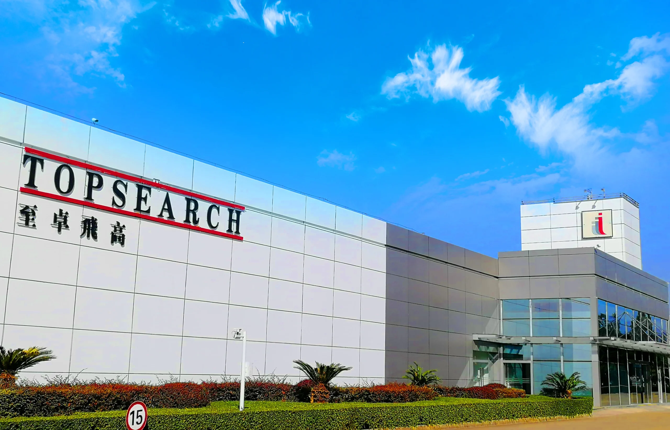
Manufacturing Facilities
Year of Mass Production:
2005
Product Range:
Double Side to 28 layer PCBs
Technology:
Heavy Copper (up to 6oz), High Frequency Materials HDI, VOP, Blind and buried Via.
Monthly Capacity:
1.5 M sq. ft
Manufacturing Facilities

Research Development
With our wealth of expertise, you can always count on us to deliver you next generation solutions.
Joint Research Projects With:

( Embedded passive components, Next generation laser drilling capability, Thermal curing resin, Ultra-fineline PCB products )

( Green Manufacturing )

About Us
Topsearch establishes in year 1985 in Hong Kong with 40 years of experience in PCB market.
Based on our board range of product type (2-18 layers ,level 3 HDI, VOP , BVH and Hybrid design)
and experience on different products segment (medical, automotive, consumer, LED, etc), we can
provide a one stop solution to our customers. Topsearch exports the products to many countries
and has high recognition on the quality of the products.

About Us
Founded in 1985, Topsearch has established itself as a pioneer in PCB manufacturing. In 1987, we set up state-of-the-art PCB manufacturing facilities in China. Our production facilities were strategically established in Shekou, Shenzhen, and commenced operations in 1988.
©Copyright 2025 by Topsearch, All rights reserved.
